AI’s copper problem just got a 3.2Tb/s optical fix—if it works
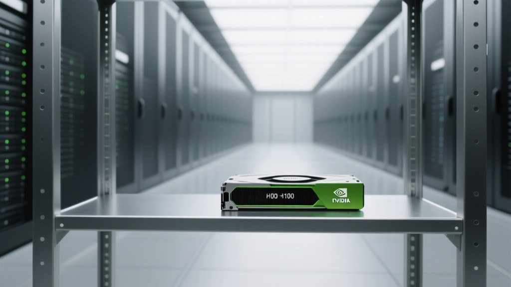
A single Nvidia H100 GPU unit sitting small and isolated on a metal shelf within a massive, cavernous data center hall stretching into the distance,📷 Photo by Tech&Space
- ★Nvidia, AMD, Meta bypass copper with 3.2Tb/s optical PHY
- ★Standardized interconnects could cut AI cluster costs by 30%
- ★Real-world adoption hinges on ecosystem lock-in risks
The Optical Compute Interconnect MSA isn’t just another industry consortium. It’s a rare alignment of rivals—Nvidia, AMD, Microsoft, Broadcom, and Meta—united by a shared pain point: copper cabling can’t keep up with AI’s data hunger. Current high-end GPUs like Nvidia’s H100 already hit bottlenecks moving training data between racks, and the problem scales exponentially with model size. Optical interconnects promise to replace copper’s 800Gb/s limits with 3.2Tb/s throughput, but the real test isn’t raw speed—it’s whether this becomes the default plumbing for next-gen clusters.
The alliance’s focus on a standardized PHY layer (the physical interface between chips and cables) is the smart play. Unlike proprietary solutions from companies like Ayar Labs, this MSA aims for multi-vendor compatibility—meaning data centers could mix AMD and Nvidia hardware without rewiring. Early adopters like Meta, which runs some of the world’s largest AI training clusters, stand to gain the most. But the catch? Optical components still cost 2–3x more than copper, and the savings from reduced power/cooling need to outweigh that premium.
This isn’t about replacing Ethernet or InfiniBand overnight. It’s about solving the ‘last meter’ problem: the short, high-bandwidth links between GPUs, switches, and storage that copper struggles with at scale. The MSA’s technical specs suggest a modular design, but real-world deployment will hinge on whether cloud providers—AWS, Google, and Azure—adopt it or stick with their own custom solutions.

A dense ceiling-view tangle of thick copper cables overwhelming a row of identical GPU units in a cavernous data center hall stretching into the📷 Photo by Tech&Space
The spec sheet promises speed, but the data center reality is messier
For AI developers, the practical impact could be dramatic. Training large language models today often means renting thousands of GPUs for weeks, with 30–40% of costs eaten by data movement inefficiencies. A 3.2Tb/s optical link between nodes could shrink that overhead—but only if the software stack (PyTorch, JAX) and scheduling tools (Kubernetes) adapt. Early benchmarks from Broadcom’s optical prototypes show latency improvements, but real-world gains depend on how well the MSA’s standard plays with existing data center architectures.
The bigger question is whether this becomes an industry standard or just another niche solution. Copper’s dominance persists because it’s cheap, familiar, and ‘good enough’ for most workloads. Optical’s advantage only becomes clear at extreme scales—think Meta’s 10,000-GPU clusters, not your average startup’s fine-tuning jobs. And while the MSA’s backers are heavyweights, notable absences (Intel, AWS, Google) could fragment adoption. If history repeats, we might see a repeat of the Gen-Z consortium’s struggles: a technically sound standard that fails to displace incumbents.
Then there’s the ecosystem tax. Optical interconnects require new cables, transceivers, and potentially even GPU designs. Data centers built for copper won’t upgrade overnight—if ever. The MSA’s success hinges on proving that the total cost of ownership (capital expenditure + operational savings) beats copper over a 3–5 year horizon. For hyperscalers, that math might work. For everyone else? It’s still a gamble.