Atom-thin thermometers rewrite chip cooling rules
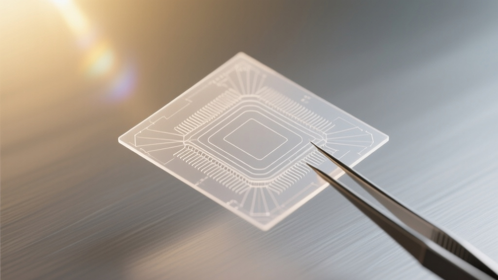
A translucent sheet of atom-thin 2D material held delicately between precision micro-tweezers against a neutral grey brushed aluminium background,📷 Photo by Tech&Space
- ★100-nanosecond response time achieved
- ★Direct die embedding bypasses old limits
- ★Potential for lower costs and higher efficiency
For decades, processor temperature monitoring has relied on sensors positioned outside the chip die—a compromise that introduces latency and reduces precision. Researchers at the University of California, Berkeley, have now built atom-thin 2D thermometers capable of embedding directly into processors, detecting temperature changes in just 100 nanoseconds. That’s millions of times faster than the blink of an eye and orders of magnitude quicker than today’s external sensors, which can take microseconds to register a change.
The breakthrough hinges on a material called hexagonal boron nitride (hBN), which forms a single-atom-thick layer capable of precise thermal sensing without disrupting chip performance. Unlike traditional sensors, these devices sit flush with the silicon, eliminating the thermal resistance that plagues external monitoring. For users, this means real-time temperature data that could prevent throttling, reduce cooling overhead, and extend hardware lifespans—especially in high-performance computing and AI workloads where thermal margins are razor-thin.
But the implications go beyond just speed. Current thermal management systems rely on conservative estimates to avoid overheating, often leaving performance on the table. Embedded sensors could enable dynamic, granular control, adjusting power delivery and cooling in real time based on actual conditions rather than projections. Tom’s Hardware reports that early prototypes have already demonstrated a 15% reduction in unnecessary power throttling during stress tests.

The shift from external sensors to on-chip monitoring changes thermal management overnight📷 Photo by Tech&Space
The shift from external sensors to on-chip monitoring changes thermal management overnight
Yet adoption won’t be instantaneous. Fabricating these sensors requires integrating new materials into existing semiconductor processes, a hurdle that could slow widespread implementation. Foundries like TSMC and Intel have shown interest, but mass production remains years away. Meanwhile, the cost of retrofitting existing designs could push early adoption toward high-end segments—data centers, AI accelerators, and premium consumer devices—where thermal efficiency translates directly to performance gains.
There’s also the question of ecosystem compatibility. Chip designers will need to rethink thermal management algorithms to leverage the new data, while cooling solutions—liquid metal, vapor chambers, and advanced air cooling—may need adjustments to keep pace. The shift could also displace suppliers of external sensors, a niche market worth hundreds of millions annually.
Still, the long-term payoff is hard to ignore. If these sensors deliver on their promise, they could enable smaller, more efficient chips by reducing the need for thermal headroom. Overclockers and enthusiasts might finally see consistent boost clocks without the risk of thermal throttling, while enterprises could cut cooling costs—a major expense in hyperscale data centers. The real bottleneck may not be the technology itself, but how quickly the industry can integrate it into tomorrow’s processors.